More 1961 - 1969 Lincoln Continentals

More 1961 - 1969 Lincoln Continentals
More Posts from Sleepysneezeydopeydoc-blog and Others

BeerBellyBlunt


“We are analog beings living in a digital world, facing a quantum future.” Neil Turok
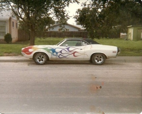

The best vintage cars, hot rods, and kustoms
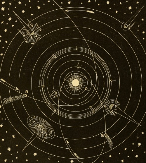
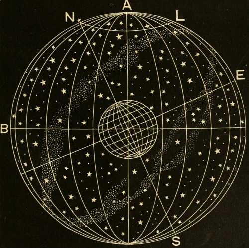
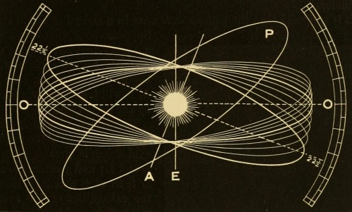
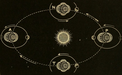
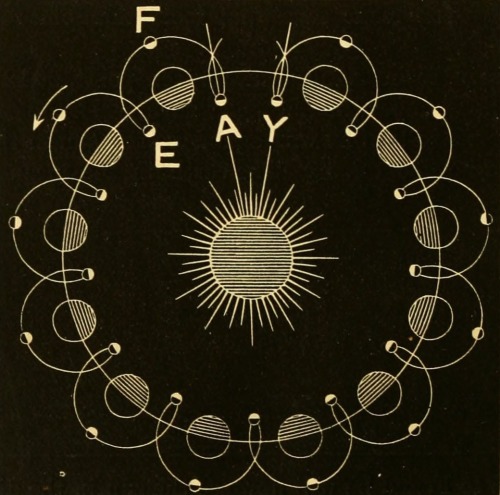
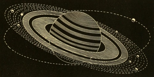
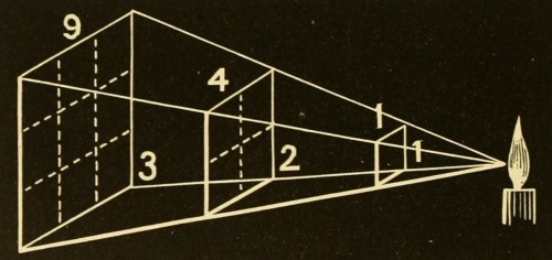
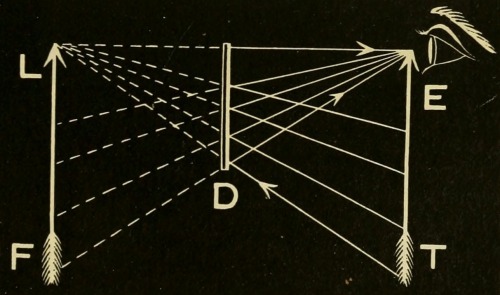
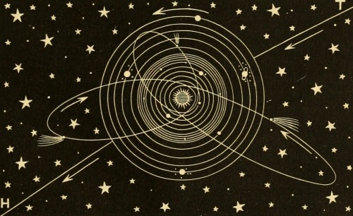
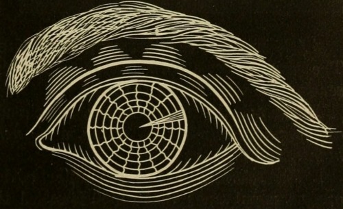
Frank G. Johnson. Solar System, Celestial and Terrestrial Latitude, The Ecliptic, Spring and Neap Tides, The Moon’s Path Around the Sun, Saturn’s Rings, Intensity of Light at Different Distances, The Optics of Plane Mirrors, The Orbit of the Sun, Method of Adjusting the Pupil or Aperture of the Eye. Johnson’s Natural Philosophy, and Key to Philosophical Charts. 1872.

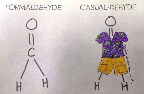
Dunno if it has happened, but it’s accurate

Stenciling with atoms in 2-dimensional materials possible
The possibilities for the new field of two-dimensional, one-atomic-layer-thick materials, including but not limited to graphene, appear almost limitless. In new research, Penn State material scientists report two discoveries that will provide a simple and effective way to “stencil” high-quality 2D materials in precise locations and overcome a barrier to their use in next-generation electronics.
In 2004, the discovery of a way to isolate a single atomic layer of carbon – graphene – opened a new world of 2D materials with properties not necessarily found in the familiar 3D world. Among these materials are a large group of elements – transition metals – that fall in the middle of the periodic table. When atoms of certain transition metals, for instance molybdenum, are layered between two layers of atoms from the chalcogenide elements, such as sulfur or selenium, the result is a three-layer sandwich called a transition metal dichalcogenide. TMDs have created tremendous interest among materials scientists because of their potential for new types of electronics, optoelectronics and computation.
Read more.

-
 billck01 reblogged this · 9 months ago
 -
 le-magicien-rouge liked this · 9 months ago
 -
 newtalot liked this · 9 months ago
 -
 sins1987 liked this · 9 months ago
 -
 dfmvluc liked this · 9 months ago
 -
 normalisboring-42 liked this · 9 months ago
 -
 massivetyphoonflower liked this · 9 months ago
 -
vdubbloke liked this · 9 months ago
-
 phatvegan reblogged this · 9 months ago
 -
phatvegan liked this · 9 months ago
-
 somestinkydude liked this · 9 months ago
 -
 hairyhotandnakeddesert liked this · 9 months ago
 -
 drmwa46 liked this · 9 months ago
 -
 viktorvochalin reblogged this · 9 months ago
 -
 ratroddermetal liked this · 9 months ago
 -
 suicideslabs reblogged this · 9 months ago
 -
 viernuleen401 liked this · 1 year ago
 -
 blogwelberfotos-blog liked this · 1 year ago
 -
 hued-man-power liked this · 1 year ago
 -
midniteman liked this · 1 year ago
-
 johnny5321 liked this · 1 year ago
 -
suicideslabs reblogged this · 1 year ago
-
 jmncamacho liked this · 1 year ago
 -
 pjsprawling liked this · 1 year ago
 -
 darriusnard liked this · 1 year ago
 -
 thesoftersideofme reblogged this · 1 year ago
 -
 plumbercrackus3 liked this · 1 year ago
 -
 phatone101 liked this · 1 year ago
 -
suicideslabs reblogged this · 1 year ago
-
 formvomar liked this · 1 year ago
 -
 speedmaster302 liked this · 1 year ago
 -
thirteenblackrainbows liked this · 1 year ago
-
2004zx6r liked this · 1 year ago
-
suicideslabs reblogged this · 1 year ago
-
csaintsfan2526 liked this · 2 years ago